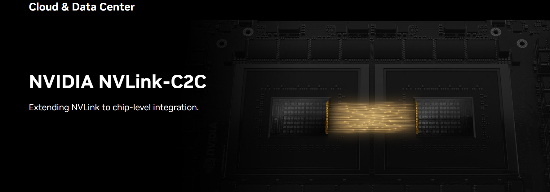
Ultra-Fast Chip Interconnect Technology for Custom Silicon Integration
NVIDIA® NVLink®-C2C extends the industry-leading NVLink technology to a chip-to-chip interconnect. This enables the creation of a new class of integrated products with NVIDIA partners, built via chiplets, allowing NVIDIA GPUs, DPUs, and CPUs to be coherently interconnected with custom silicon.
Building Semi-Custom Chip Designs
The design and layout of a chip-to-chip interconnect is vital to proper function, performance, power efficiency, reliability, and fabrication yield. NVIDIA NVLink-C2C is built on top of the world-class SerDes and Link design technology. With advanced packaging, NVLink-C2C interconnect delivers up to 25X more energy efficiency and 90X more area-efficiency than a PCIe Gen 5 PHY on NVIDIA chips. NVLink-C2C is extensible from PCB-level integration, multi-chip modules (MCM), and silicon interposer or wafer-level connections, enabling the industry’s highest bandwidth, while optimizing for both energy and area efficiency. The NVLink-C2C technology will be available for customers and partners who want to create semi-custom system designs.
Products Using NVLink-C2C
NVIDIA GB200 NVL72
NVIDIA Grace Hopper Superchip
NVIDIA Grace CPU Superchip
NVLink-C2C Benefits
High Bandwidth
Supports high-bandwidth coherent data transfers between processors and accelerators.
Low Latency
Supports atomics between processors and accelerators to perform fast synchronization and high-frequency updates to shared data.
Low-Power High Density
Uses advanced packaging to deliver 25X more energy efficiency and 90X more area-efficiency than PCIe Gen 5 PHY on NVIDIA chips.
Industry Standards
Supports Arm’s AMBA CHI (Coherent Hub Interface) or Compute Express Link (CXL) industry standard protocols for interoperability between devices.

 MacBook
 iPad
iPad Apple Watch
 Airpods
 iMac
iMac Studio Display
 iphone
 Gaming Laptop
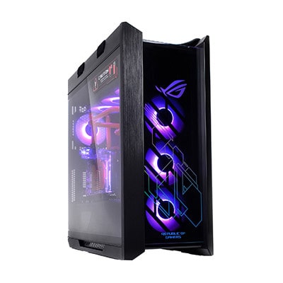
 Gaming Desktop
 DDR5 Desktop
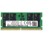 DDR5 Laptop
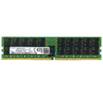 DDR5 Server
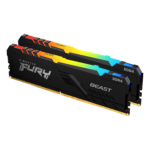 DDR4 Desktop
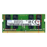 DDR4 Laptop
 DDR4 Server
 DDR3 Desktop
 DDR3 Laptop
 DDR3 Server
 Intel Socket
 Intel Z890
 Intel B860
 Intel B760
 Intel H770
 Intel B660
 Intel H670
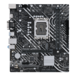 Intel H610
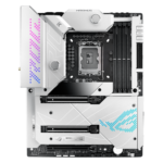 Intel Z690
 Intel H510
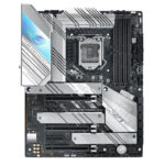 Intel Z590
 Intel B560
 Intel H470
 Intel Z490
 Intel H410
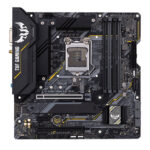 Intel B460
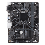 Intel H310
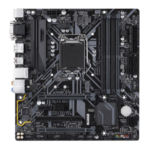 Intel B360
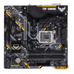 Intel B365
 Intel X299
 Intel Z390
 Intel Z370
 Intel H370
 Intel Z270 H270
 Intel B250
 Intel Z170 H170
 Intel H110
 Intel H81
 Intel B85
 Intel H61
 Intel B150
 AMD Socket
 AMD B850
 AMD B840
 AMD TRX50
 AMD A620
 AMD X870
 AMD B650
 AMD A520
 AMD TRX40
 AMD B550
 AMD X570
 AMD X470
 AMD B450
 AMD X370
 AMD A320
 AMD B350
 AMD X399
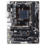 AMD A88
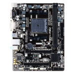 AMD A68 A78
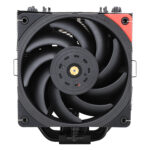 Cpu Air Coolers
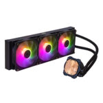 CPU Liquid Coolers
 Fans
Fans
 AMD CPUs Desktop
 AMD Server CPU
 Intel Server CPU
 Samsung CPUs
 Other special CPUs

 Solid State Drives
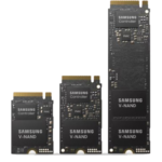 NVMe PCIe M.2
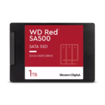 SATA 2.5inch
 Hard Disk Drive
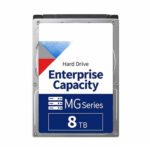 Server Hard Drives
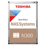 NAS hard drive
 Monitoring hard drive
 Portable Solid State Drives
 Memory Cards
 USB Flash Drives
 Nvidia GPU
 RTX 50 series
 RTX 30 series
 GTX 16 series
 GTX 10 series
 RX 9000 series
 RX 7000 series
 RX 6000 series
 RX 5000 series
 RX 500 series
 RTX 20 series
 Rack server
 Blade server
 Tower server
 Storage Server Solutions
 Network switch
 Workstation
 Mobile Workstation
 Server motherboard
 Workstation Motherboard
PSP3000索尼原装街机掌机-150x150.jpg) SONY Gaming Console
SONY Gaming Console ASUS Gaming Console
Legion-Go-游戏掌机手持设备-150x150.jpg) Lenovo Gaming Console
Lenovo Gaming Console One XPlayer
日版-Xbox-Series-X-XSX次世代-150x150.jpg) Microsoft Gaming Console
Microsoft Gaming Console XBOX Gaming Console
MSI-Claw-A1M-050US-游戏掌机-150x150.jpg) MSI Gaming Console
MSI Gaming Console
 Motherboard
 GTX TITAN
 Computer Cases